- 您现在的位置:买卖IC网 > Sheet目录334 > ISL6622CBZ-T (Intersil)IC MOSFET DVR SYNC BUCK 8-SOIC
�� �
�
�ISL6622�
�Gate� Voltage� Optimization� Technology� (GVOT)�
�The� ISL6622� provides� the� user� flexibility� in� choosing� the�
�gate� drive� voltage� for� efficiency� optimization.� During� light�
�load� operation,� the� switching� losses� dominate� system�
�performance.� Dropping� down� to� a� lower� drive� voltage� with�
�GVOT� during� light� load� operation� can� reduce� the� switching�
�losses� and� maximize� system� efficiency.�
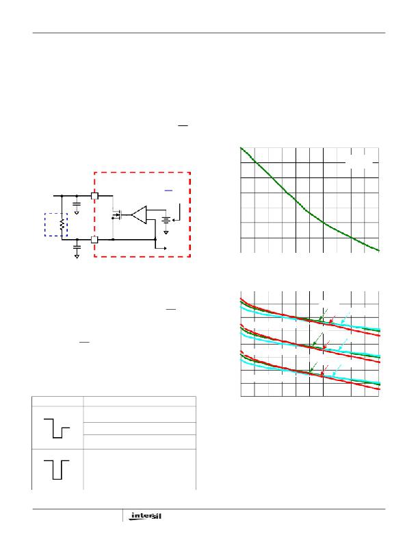
�Figure� 2� shows� that� the� gate� drive� voltage� optimization� is�
�accomplished� via� an� internal� low� drop� out� regulator� (LDO)�
�that� regulates� the� lower� gate� drive� voltage.� LVCC� is� driven� to�
�a� lower� voltage� depending� on� the� state� of� the� internal� PSI�
�signal� and� the� GD_SEL� pin� impedance.� The� input� and�
�output� of� this� internal� regulator� is� the� VCC� and� LVCC� pins,�
�Figure� 3� illustrates� the� internal� LDO’s� variation� with� the�
�average� load� current� plotted� over� a� range� of� temperatures�
�spanning� from� -40� °� C� to� +120� °� C.� Should� finer� tweaking� of� this�
�LVCC� voltage� be� necessary,� a� resistor� (R� CC� )� can� be� used� to�
�shunt� the� LDO,� as� shown� in� Figure� 2.� The� resistor� delivers�
�part� of� the� LGATE� drive� current,� leaving� less� current� going�
�through� the� internal� LDO,� elevating� the� LDO’s� output�
�voltage.� Further� reduction� in� RCC’s� value� can� raise� the�
�LVCC� voltage� further,� as� desired.�
�Figure� 4� also� details� the� typical� LDO� performance� when� the�
�pass� element� is� fully� enhanced,� as� it� is� the� case� when� the�
�driver� operates� in� CCM.�
�12.0�
�respectively.� Both� VCC� and� LVCC� should� be� decoupled� with�
�a� high� quality� low� ESR� ceramic� capacitor.�
�11.8�
�VCC� =� 12V�
�+40°C�
�EXTERNAL� CIRCUIT�
�ISL6622� INTERNAL� CIRCUIT�
�SET� BY�
�11.6�
�VIN� >�
�RCC�
�VCC�
�1μF�
�GVOT�
�LDO�
�+�
�-�
�PSI� AND�
�GD_SEL�
�+�
�-�
�11.4�
�11.2�
�11.0�
�LVCC�
�LGATE�
�10.8�
�1μF�
�DRIVER�
�10.6�
�0�
�20�
�40�
�60�
�80�
�100�
�RCC� =� OPTION� FOR� HIGHER� LVCC�
�THAN� PRE-SET� BY� GD_SEL�
�AVERAGE� LOAD� CURRENT� (mA)�
�FIGURE� 3.� TYPICAL� LVCC� VARIATION� WITH� LOAD� (CCM)�
�FIGURE� 2.� GATE� VOLTAGE� OPTIMIZATION� (GVOT)� DETAIL�
�9.0�
�In� the� 8� Ld� SOIC� package,� the� ISL6622� drives� the� upper� and�
�lower� gates� close� to� VCC� during� normal� PWM� mode,� while�
�8.5�
�+40°C�
�the� lower� gate� drops� down� to� a� fixed� 5.75V� during� PSI� mode.�
�The� 10� Ld� DFN� part� offers� more� flexibility:� the� upper� gate� can�
�be� driven� from� 5V� to� 12V� via� the� UVCC� pin,� while� the� lower�
�8.0�
�7.5�
�GD_SEL TIED TO GND�
�+40°C�
�+120°C�
�-40°C�
�gate� has� a� resistor-selectable� drive� voltage� of� 5.75V,� 6.75V,�
�+120°C�
�-40°C�
�and� 7.75V� during� PSI� mode.� This� provides� the� flexibility�
�necessary� to� optimize� applications� involving� trade-offs�
�between� gate� charge� and� conduction� losses.� Table� 1� shows�
�the� LDO� output� (LVCC)� level� set� by� the� PWM� input� and�
�GD_SEL� pin� impedance.�
�7.0�
�6.5�
�6.0�
�5.5�
�GD_SEL 4.5k� Ω� TO GND�
�GD_SEL FLOATING�
�+40°C�
�+120°C� -40°C�
�TABLE� 1.� LDO� OPERATION� AND� OPTIONS�
�PWM� INPUT�
�GD_SEL� PIN�
�LVCC� @� 50mA� DC� LOAD�
�5.0�
�0�
�20�
�40� 60� 80�
�100�
�5V�
�0V�
�2� .5� V�
�Floating�
�4.5k� Ω� to� GND�
�GND�
�5.75V� (Typical;� Fixed� in�
�SOIC� Package)�
�6.75V� (Typical)�
�7.75V� (Typical)�
�AVERAGE� LOAD� CURRENT� (mA)�
�FIGURE� 4.� TYPICAL� LVCC� VARIATION� WITH� LOAD� (DEM)�
�Power-On� Reset� (POR)� Function�
�During� initial� start-up,� the� VCC� voltage� rise� is� monitored.�
�Once� the� rising� VCC� voltage� exceeds� rising� POR� threshold,�
�5V�
�DON’T� CARE�
�11.20V� (Typical)�
�operation� of� the� driver� is� enabled� and� the� PWM� input� signal�
�takes� control� of� the� gate� drives.� If� VCC� drops� below� the� POR�
�falling� threshold,� operation� of� the� driver� is� disabled.�
�0V�
�7�
�FN6470.2�
�October� 30,� 2008�
�发布紧急采购,3分钟左右您将得到回复。
相关PDF资料
ISL6801ABT
IC DRIVER HISIDE BOOTSTRAP 8SOIC
ISL78100ARZ
IC LED DRIVER AUTOMOTIVE 20-QFN
ISL8013AEVAL2Z
EVAL BOARD 2 FOR ISL8013A
ISL8014AEVAL2Z
EVAL BOARD 2 FOR ISL8014A
ISL8022EVAL2Z
EVAL BOARD 2 FOR ISL8023
ISL8088EVAL2Z
EVAL BAORD FOR ISL8088
ISL8105BEVAL2Z
EVALUATION BOARD FOR ISL8105B
ISL8112EVAL1Z
EVALUATION BOARD FOR ISL8112
相关代理商/技术参数
ISL6622CRZ
功能描述:IC MOSFET DRVR SYNC BUCK 10-DFN RoHS:是 类别:集成电路 (IC) >> PMIC - MOSFET,电桥驱动器 - 外部开关 系列:- 标准包装:6,000 系列:*
ISL6622CRZ-T
功能描述:IC MOSFET DVR SYNC BUCK 10-DFN RoHS:是 类别:集成电路 (IC) >> PMIC - MOSFET,电桥驱动器 - 外部开关 系列:- 标准包装:95 系列:- 配置:半桥 输入类型:PWM 延迟时间:25ns 电流 - 峰:1.6A 配置数:1 输出数:2 高端电压 - 最大(自引导启动):118V 电源电压:9 V ~ 14 V 工作温度:-40°C ~ 125°C 安装类型:表面贴装 封装/外壳:8-SOIC(0.154",3.90mm 宽) 供应商设备封装:8-SOIC 包装:管件 产品目录页面:1282 (CN2011-ZH PDF) 其它名称:*LM5104M*LM5104M/NOPBLM5104M
ISL6622IBZ
功能描述:IC MOSFET DRVR SYNC BUCK 8-SOIC RoHS:是 类别:集成电路 (IC) >> PMIC - MOSFET,电桥驱动器 - 外部开关 系列:- 标准包装:50 系列:- 配置:高端 输入类型:非反相 延迟时间:200ns 电流 - 峰:250mA 配置数:1 输出数:1 高端电压 - 最大(自引导启动):600V 电源电压:12 V ~ 20 V 工作温度:-40°C ~ 125°C 安装类型:通孔 封装/外壳:8-DIP(0.300",7.62mm) 供应商设备封装:8-DIP 包装:管件 其它名称:*IR2127
ISL6622IBZ-T
功能描述:IC MOSFET DRVR SYNC BUCK 8-SOIC RoHS:是 类别:集成电路 (IC) >> PMIC - MOSFET,电桥驱动器 - 外部开关 系列:- 标准包装:50 系列:- 配置:高端 输入类型:非反相 延迟时间:200ns 电流 - 峰:250mA 配置数:1 输出数:1 高端电压 - 最大(自引导启动):600V 电源电压:12 V ~ 20 V 工作温度:-40°C ~ 125°C 安装类型:通孔 封装/外壳:8-DIP(0.300",7.62mm) 供应商设备封装:8-DIP 包装:管件 其它名称:*IR2127
ISL6622IRZ
功能描述:IC MOSFET DRVR SYNC BUCK 10-DFN RoHS:是 类别:集成电路 (IC) >> PMIC - MOSFET,电桥驱动器 - 外部开关 系列:- 标准包装:50 系列:- 配置:高端 输入类型:非反相 延迟时间:200ns 电流 - 峰:250mA 配置数:1 输出数:1 高端电压 - 最大(自引导启动):600V 电源电压:12 V ~ 20 V 工作温度:-40°C ~ 125°C 安装类型:通孔 封装/外壳:8-DIP(0.300",7.62mm) 供应商设备封装:8-DIP 包装:管件 其它名称:*IR2127
ISL6622IRZ-T
功能描述:IC MOSFET DRVR SYNC BUCK 10-DFN RoHS:是 类别:集成电路 (IC) >> PMIC - MOSFET,电桥驱动器 - 外部开关 系列:- 标准包装:50 系列:- 配置:高端 输入类型:非反相 延迟时间:200ns 电流 - 峰:250mA 配置数:1 输出数:1 高端电压 - 最大(自引导启动):600V 电源电压:12 V ~ 20 V 工作温度:-40°C ~ 125°C 安装类型:通孔 封装/外壳:8-DIP(0.300",7.62mm) 供应商设备封装:8-DIP 包装:管件 其它名称:*IR2127
ISL6625ACRZ
制造商:Intersil 功能描述:Synchronous Rectified Buck MOSFET Drivers
ISL6625ACRZ-T
制造商:Intersil Corporation 功能描述:LEAD-FREE VERSION OF ISL6625A 8LD DFN 2 X 2 - Tape and Reel 制造商:Intersil Corporation 功能描述:IC MOSFET DRVR SYNCH RECT 8DFN 制造商:Intersil 功能描述:Synch. Rect. Buck MOSFET Driver